Semiconductors

JEE Main level, single correct, medium

59 of 209

Question 59 of 209

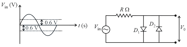
In the given circuit the input voltage Vin{V}_{in} is shown in figure. The cut-in voltage of p−np-n junction diode (D1{D}_{1} or D2{D}_{2}) is 0.6V0.6V. Which of the following output voltage (V0)\left({V}_{0}\right) waveform across the diode is correct?

Show answer and solution

Answer: (D)
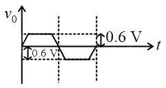
During the positive half cycle of the input waveform, diode D1{D}_{1} is forward biased and diode D2{D}_{2} is reverse biased. Here 0.6V0.6V appears across the output as the diode is conducting. During negative half cycle the diode D1{D}_{1} is reverse biased and D2{D}_{2} is forward biased, so, −0.6V-0.6V appears across the output as the diode is conducting in negative direction. This circuit can be used as a voltage limiter. This circuit will not allow any voltage above 0.6V0.6Vand below −0.6V-0.6V.
Hence, the output waveform is

JEE Main question paper PDF

Open a shift to read the full paper on this page, or download it.

JEE Main 2025 Apr 2 Shift 1 question paper

Open Download PDF

Opening paper…

Explain it as a whiteboard videoStep-by-step, in Hinglish or English. Your first video needs no login.Solved it on paper but got it wrong?Upload a photo of your working. Mistake Doctor marks the exact line that broke.
See it move: Semiconductors, diodes and logic gates simulationDrag the sliders and watch the numbers in this question change.

More Physics practice

JEE Main Physics practice question on Semiconductors (Diodes), with the answer and a step-by-step solution. Scan a question from your own book or paper to get a whiteboard video.