Physics · JEE Main, NEET
Semiconductors
209 practice questions with a worked solution for each. Tap an option to see instantly if you are right.
182MCQ27Numerical144With diagram
- 1Which of the following logic gates provides output only when both inputs and ?JEE Main/MCQ/Medium
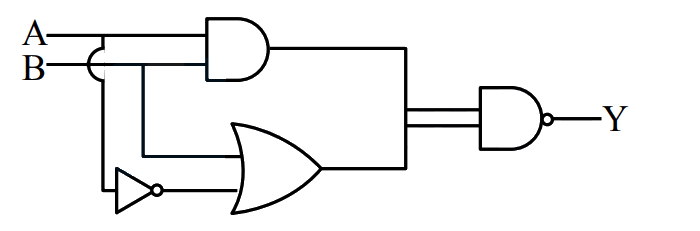
- 2In the given digital logic circuit network consisting of a NAND gate followed by a NOT gate, if inputs are and , the final output will be:NEET/MCQ/Medium/With diagram
- 3In a forward biased P-N junction diode, the depletion layer width:JEE Main/MCQ/Medium
- 4In a common emitter NPN transistor amplifier, input resistance is and load resistance is . If , voltage gain is:JEE Main/MCQ/Medium
- 5A light emitting diode (LED) is fabricated using GaAs semiconducting material whose band gap is . The wavelength of light emitted from the LED is :JEE Main/MCQ/Medium/Energy Bands in Solids
- 6The acceptor level of a p-type semiconductor is . The maximum wavelength of light which can create a hole would be : Given .JEE Main/MCQ/Medium/Energy Bands in Solids
- 7Match the List I with List II List I List II A Intrinsic Semiconductor I Fermi-level near valence band B n-type semiconductor II Fermi-level at middle of valence and conduction band C p-type semiconductor III Fermi-level near conduction band D Metals IV Fermi-level inside conduction band Choose the correct answer from the options given below:JEE Main/MCQ/Medium/Energy Bands in Solids
- 8The effect of increase in temperature on the number of electrons in conduction band and resistance of a semiconductor will be as:JEE Main/MCQ/Medium/Energy Bands in Solids
- 9The energy band gap of semiconducting material to produce violet (wavelength ) LED is _____ . (Round off to the nearest integer).JEE Main/Numerical/Medium/Energy Bands in Solids
- 10Consider a situation in which reverse biased current of a particular junction increases when it is exposed to a light of wavelength During this process, enhancement in carrier concentration takes place due to generation of hole-electron pairs. The value of band gap is nearly.JEE Main/MCQ/Medium/Energy Bands in Solids
- 11This question has Statement 1 and Statement 2. Of the four choices given after the Statements, choose the one that best describes the two Statements.
Statement 1: A pure semiconductor has negative temperature coefficient of resistance.
Statement 2: On raising the temperature, more charge carriers are released into the conduction band.JEE Main/MCQ/Medium/Energy Bands in Solids - 12If the lattice constant of this semiconductor is decreased, then which of the following is correct?
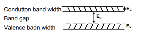 JEE Main/MCQ/Medium/Energy Bands in Solids/With diagram
- 13The electrical conductivity of a semiconductor increases when electromagnetic radiation of wavelength shorter than is incident on it. The band gap in (eV) for the semiconductor isJEE Main/MCQ/Medium/Energy Bands in Solids
- 14The energy band gap is maximum inJEE Main/MCQ/Medium/Energy Bands in Solids
- 15Consider a n-type semiconductor in which and are number of electrons and holes, respectively.
(A) Holes are minority carriers
(B) The dopant is a pentavalent atom
(C)
(where is number of electrons or holes in semiconductor when it is intrinsic form)
(D)
(E) The holes are not generated due to the donors Choose the correct answer from the options given below :JEE Main/MCQ/Medium/Semiconductors - 16Given below are two statements: one is labelled as Assertion A and the other is labelled as Reason R
Assertion A: Diffusion current in a junction is greater than the drift current in magnitude if the junction is forward biased.
Reason R: Diffusion current in a junction is form the -side to the -side if the junction is forward biased.
In the light of the above statements, choose the most appropriate answer from the options given below.JEE Main/MCQ/Medium/Semiconductors - 17The resistivity of semiconductor varies with temperature. Which of the following curve represents the correct behaviour?JEE Main/MCQ/Medium/Semiconductors
- 18Statement I : When a Si sample is doped with Boron, it becomes P type and when doped by Arsenic it becomes N-type semi conductor such that P-type has excess holes and N-type has excess electrons.
Statement II : When such P-type and N-type semi-conductors, are fused to make a junction, a current will automatically flow which can be detected with an externally connected ammeter.
In the light of above statements, choose the most appropriate answer from the options given below.JEE Main/MCQ/Medium/Semiconductors - 19Statement I: By doping silicon semiconductors with pentavalent material, the electrons density increases.
Statement II: The type of semiconductor has a net negative charge.
In the above statements, choose the most appropriate answer from the options given below:JEE Main/MCQ/Medium/Semiconductors - 20In a semiconductor, the number density of intrinsic charge carriers at is . If the semiconductor is doped with an impurity atom, the hole density increases to . The electron density in the doped semiconductor is _______JEE Main/Numerical/Medium/Semiconductors
- 21For extrinsic semiconductors; when doping level is increased;JEE Main/MCQ/Medium/Semiconductors
- 22The conductivity of a semiconductor sample having electron concentration of , hole concentration of , electron mobility of and hole mobility of is
(Take charge of an electron as )JEE Main/MCQ/Medium/Semiconductors - 23The temperature dependence of resistance of and undoped in the temperature range is best described byJEE Main/MCQ/Medium/Semiconductors
- 24Carbon, silicon and germanium have four valence electrons each. At room temperature which one of the following statements is most appropriate?JEE Main/MCQ/Medium/Semiconductors
- 25If the ratio of the concentration of electrons that of holes in a semiconductor is and the ratio of currents is , then what is the ratio of their drift velocities?JEE Main/MCQ/Medium/Semiconductors
- 26The difference in the variation of resistance with temperature in a metal and a semiconductor arises essentially due to the difference in theJEE Main/MCQ/Medium/Semiconductors
- 27At absolute zero, Si acts asJEE Main/MCQ/Medium/Semiconductors
- 28The maximum rated power of the LED is mW and it is used in the circuit with input voltage of V as shown in the figure below. The current through resistance is mA. The minimum value of the resistance of , to ensure that the LED is not damaged is _______ k.
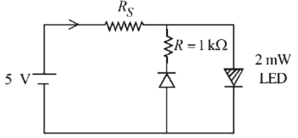 JEE Main/MCQ/Medium/Diodes/With diagram
- 29In a semiconductor p-n diode, the doping concentrations on p-side and n-side are and , respectively. Which one of the following statements is true ?JEE Main/MCQ/Medium/Diodes
- 30A diode has Zener voltage of V and maximum power dissipation of W, then the minimum resistance to be used in series with this diode for safety when it is connected to a V power supply is ______ .JEE Main/Numerical/Medium/Diodes
- 31Given below are two statements: one is labelled as Assertion A and the other is labelled as Reason R
Assertion A: A diode under reverse-biased condition provides very small current which is nearly independent of voltage until a critical limit at which the current increases drastically.
Reason R: Below the critical voltage limit, only majority charge carriers flow which increases drastically above critical voltage.
Choose the correct answer from the options given belowJEE Main/MCQ/Medium/Diodes - 32For the given circuit (shown in part (A)) the time dependent input voltage and corresponding output are shown in part (B) and part (C), respectively. Identify the components that are used in the circuit between points X and Y.
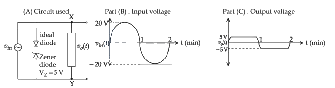 JEE Main/MCQ/Medium/Diodes/With diagram
- 33Assuming in forward bias condition there is a voltage drop of 0.7 V across a silicon diode, the current through diode in the circuit is mA.
(Assume all diodes in the given circuit are identical)
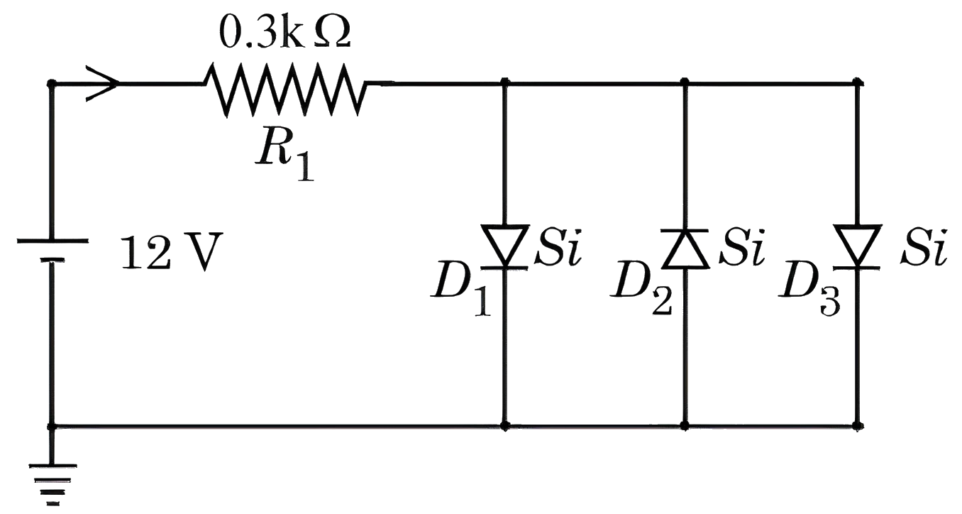 JEE Main/MCQ/Medium/Diodes/With diagram
- 34A voltage regulating circuit consisting of Zener diode, having break-down voltage of 10 V and maximum power dissipation of 0.4 W, is operated at 15 V. The approximate value of protective resistance in this circuit is .JEE Main/Numerical/Medium/Diodes
- 35The following diagram shows a Zener diode as a voltage regulator. The Zener diode is rated at and the desired current in load is 5 mA. The unregulated voltage source can supply upto 25 V. Considering the Zener diode can withstand four times of the load current, the value of resistor (shown in circuit) should be .
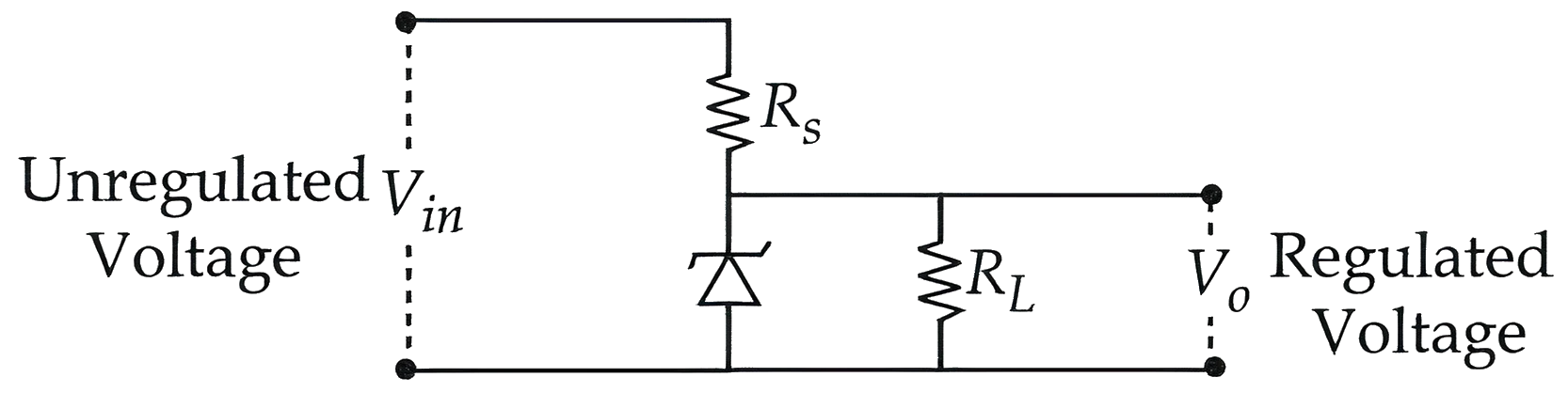 JEE Main/MCQ/Medium/Diodes/With diagram
- 36The output voltage in the following circuit is (Consider ideal diode case)
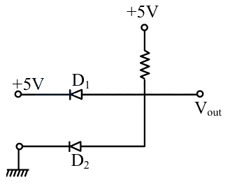 JEE Main/MCQ/Medium/Diodes/With diagram
- 37In the following circuit, the reading of the ammeter will be (Take Zener breakdown voltage
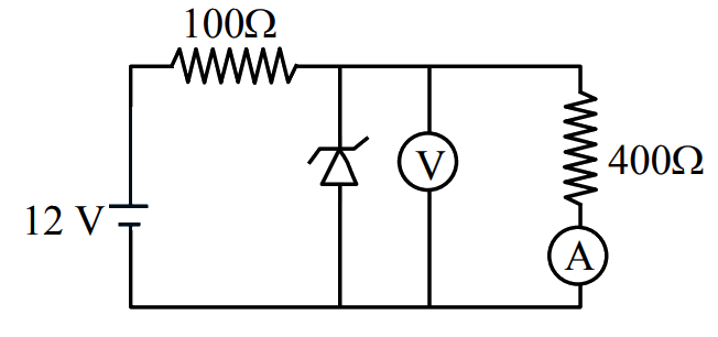 JEE Main/MCQ/Medium/Diodes/With diagram
- 38A zener diode with 5 V zener voltage is used to regulate an unregulated dc voltage input of 25 V. For a resistor connected in series, the zener current is found to be 4 times load current. The load current and load resistance are :JEE Main/MCQ/Medium/Diodes
- 39
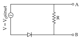
In the circuit shown here, assuming threshold voltage of diode is negligibly small, then voltage is correctly represented by :JEE Main/MCQ/Medium/Diodes/With diagram - 40Refer to the circuit diagram given in the figure. which of the following observations are correct?
A. Total resistance of circuit is
B. Current in Ammeter is 1 A
C. Potential across is 4 Volts.
D. Potential across CD is 4 Volts
E. Total resistance of the circuit is .
Choose the correct answer from the options given below: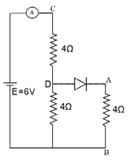 JEE Main/MCQ/Medium/Diodes/With diagram
- 41Which of the following circuits represents a forward biased diode?
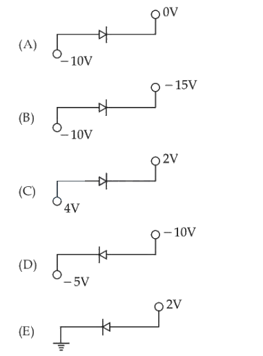
Choose the correct answer from the options given below :JEE Main/MCQ/Medium/Diodes/With diagram - 42A potential divider circuit is connected with a dc source of , a light emitting diode of glow in voltage and a zener diode of breakdown voltage of . The length (PR) of the resistive wire is . The minimum length of PQ to just glow the LED is _____
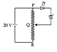 JEE Main/Numerical/Medium/Diodes/With diagram
- 43Which of the diode circuit shows correct biasing used for the measurement of dynamic resistance of p-n junction diode :JEE Main/MCQ/Medium/Diodes
- 44The value of net resistance of the network as shown in the given figure is :
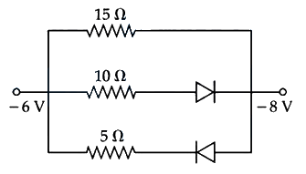 JEE Main/MCQ/Medium/Diodes/With diagram
- 45In the given circuit if the power rating of Zener diode is , the value of series resistance to regulate the input unregulated supply is:
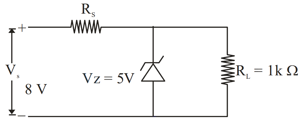 JEE Main/MCQ/Medium/Diodes/With diagram
- 46In the given circuit, the voltage across load resistance is:
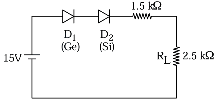 JEE Main/MCQ/Medium/Diodes/With diagram
- 47A Zener diode of breakdown voltage is used as a voltage regulator as shown in the figure. The current through the Zener diode is
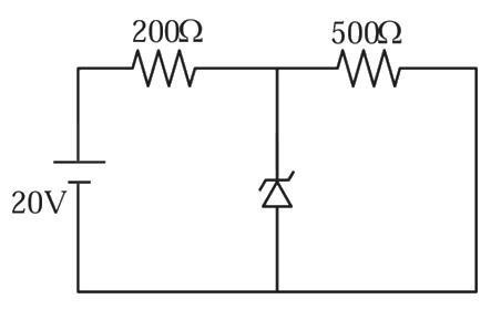 JEE Main/MCQ/Medium/Diodes/With diagram
- 48In the given circuit, the breakdown voltage of the Zener diode is . What is the value of ?
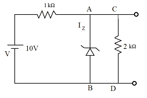 JEE Main/MCQ/Medium/Diodes/With diagram
- 49Which of the following circuits is reverse - biased ?JEE Main/MCQ/Medium/Diodes
- 50If each diode has a forward bias resistance of in the below circuit,
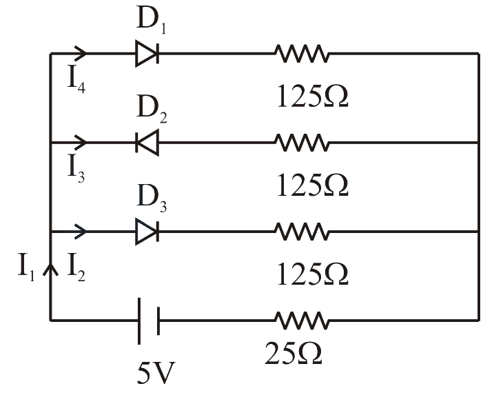
Which of the following options is correct?JEE Main/MCQ/Medium/Diodes/With diagram - 51A zener diode of power rating is to be used as voltage regulator. If the zener diode has a breakdown of and it has to regulate voltage fluctuating between and The value of resistance for safe operation of diode will be
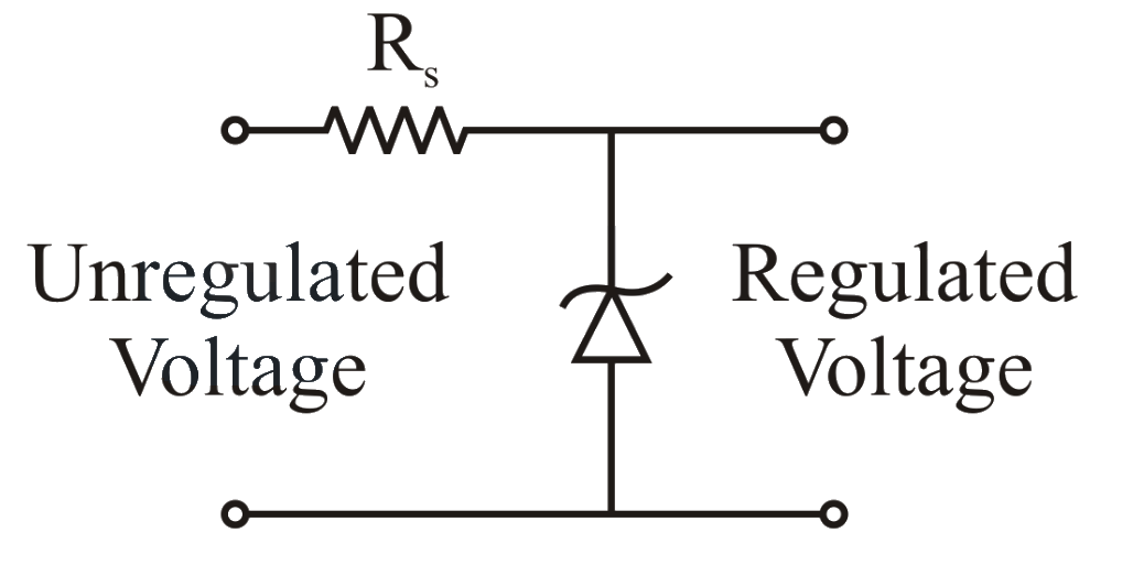 JEE Main/MCQ/Medium/Diodes/With diagram
- 52Choose the correct statement about Zener diode:JEE Main/MCQ/Medium/Diodes
- 53A Zener diode along with a series resistance is connected across a supply (as shown in the figure). If the maximum Zener current is , then the minimum value of will be _____ .
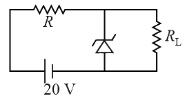 JEE Main/Numerical/Medium/Diodes/With diagram
- 54If the potential barrier across a junction is . Then the electric field intensity, in the depletion region having the width of , will be _____ JEE Main/Numerical/Medium/Diodes
- 55In the circuit shown below, maximum Zener diode current will be _____ .
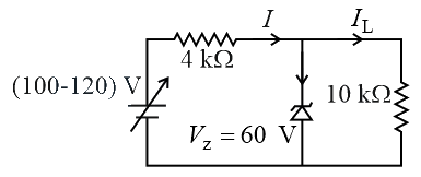 JEE Main/Numerical/Medium/Diodes/With diagram
- 56Two ideal diodes are connected in the network as shown in figure. The equivalent resistance between and is _____
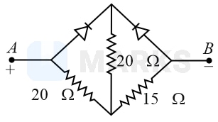 JEE Main/Numerical/Medium/Diodes/With diagram
- 57A potential barrier of exists across a p-n junction. An electron enters the junction from the -side with a speed of . The speed with which electron enters the side will be , then the value of is _____.: (Given mass of electron , charge on electron .)JEE Main/Numerical/Medium/Diodes
- 58A Zener of breakdown voltage and maximum Zener current, is subjected to an input voltage with series resistance . In the given circuit represents the variable load resistance. The ratio of maximum and minimum value of is _____ .
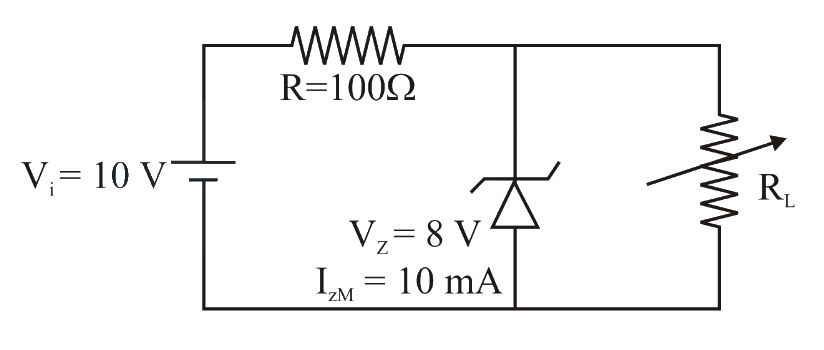 JEE Main/Numerical/Medium/Diodes/With diagram
- 59In the given circuit the input voltage is shown in figure. The cut-in voltage of junction diode ( or ) is . Which of the following output voltage waveform across the diode is correct?
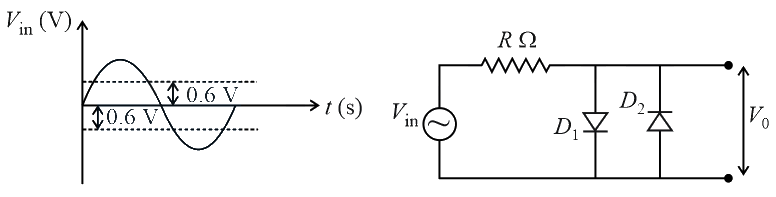 JEE Main/MCQ/Medium/Diodes/With diagram
- 60For using a multimeter to identify diode from electrical components, choose the correct statement out of the following about the diodeJEE Main/MCQ/Medium/Diodes
- 61The cut-off voltage of the diodes (shown in figure) in forward bias is . The current through the resister of is _____ .
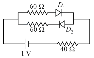 JEE Main/Numerical/Medium/Diodes/With diagram
- 62As per the given circuit, the value of current through the battery will be _____ A.
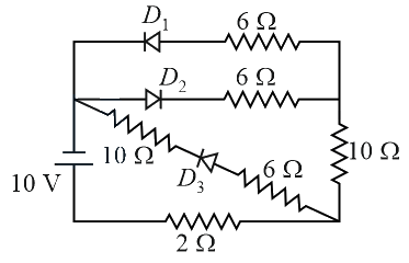 JEE Main/Numerical/Medium/Diodes/With diagram
- 63The characteristics of a junction diode in forward bias is shown in the figure. The ratio of dynamic resistance, corresponding to forward bias voltage of and respective is
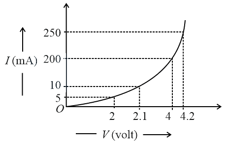 JEE Main/MCQ/Medium/Diodes/With diagram
- 64In the given circuit, the value of current will be _____ (When )
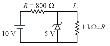 JEE Main/Numerical/Medium/Diodes/With diagram
- 65In the given figure, each diode has a forward bias resistance of and infinite resistance in reverse bias. The current will be :
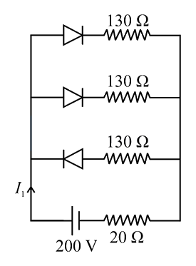 JEE Main/MCQ/Medium/Diodes/With diagram
- 66If and are the input voltages (either or ) and is the output voltage then the two gates represented in the following circuits and are :
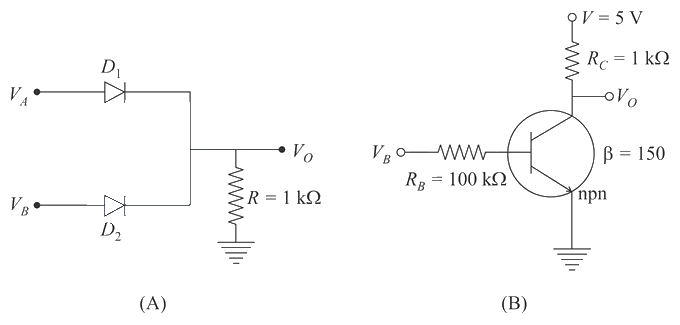 JEE Main/MCQ/Medium/Diodes/With diagram
- 67Choose the correct waveform that can represent the voltage across of the following circuit, assuming the diode is ideal one:
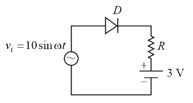 JEE Main/MCQ/Medium/Diodes/With diagram
- 68A zener diode of power rating is to be used as a voltage regulator. If the zener diode has a breakdown of and it has to regulate voltage fluctuated between and , the value of for safe operation should be _____ .
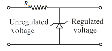 JEE Main/Numerical/Medium/Diodes/With diagram
- 69A circuit is arranged as shown in figure. The output voltage is equal to __________
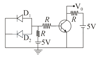 JEE Main/Numerical/Medium/Diodes/With diagram
- 70For the given circuit, the power across zener diode is _____ .
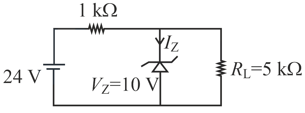 JEE Main/Numerical/Medium/Diodes/With diagram
- 71In a given circuit diagram, a zener diode along with a series resistance is connected across a power supply. The minimum value of the resistance required, if the maximum zener current is will be
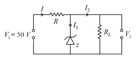 JEE Main/Numerical/Medium/Diodes/With diagram
- 72For the forward biased diode characteristics shown in the figure, the dynamic resistance at will be ________
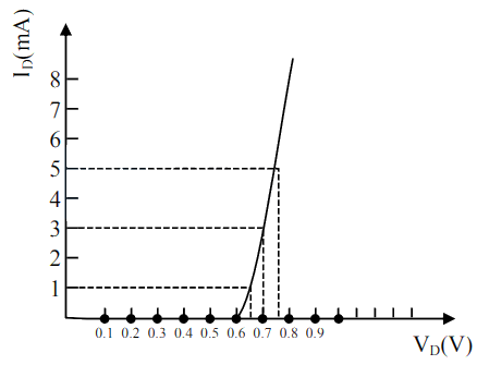 JEE Main/Numerical/Medium/Diodes/With diagram
- 73A zener diode having zener voltage and power dissipation rating of is connected across a potential divider arranged with maximum potential drop across zener diode is as shown in the diagram. The value of protective resistance is _____
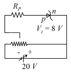 JEE Main/Numerical/Medium/Diodes/With diagram
- 74For the circuit shown below, calculate the value of
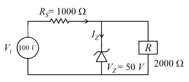 JEE Main/MCQ/Medium/Diodes/With diagram
- 75The value of power dissipated across the zener diode connected in the circuit as shown in the figure is .
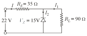
The value of to the nearest integer is _______.JEE Main/Numerical/Medium/Diodes/With diagram - 76The zener diode has a . The current passing through the diode for the following circuit is___
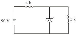 JEE Main/Numerical/Medium/Diodes/With diagram
- 77The circuit contains two diodes each with a forward resistance of and with infinite reverse resistance. If the battery voltage is , the current through the resistance is _______
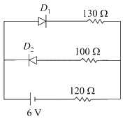 JEE Main/Numerical/Medium/Diodes/With diagram
- 78A battery is connected across the points and . Assume and to be normal silicon diodes. Find the current supplied by the battery if the terminal of the battery is connected to point .
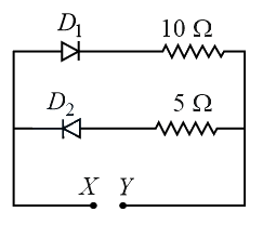 JEE Main/MCQ/Medium/Diodes/With diagram
- 79Given below are two statements:
Statement I : junction diodes can be used to function as a transistor, simply by connecting two diodes, back to back, which acts as the base terminal
Statement II: In the study of transistors, the amplification factor indicates ratio of the collector current to the base current.
In the light of the above statements, choose the correct answer from the options given below.JEE Main/MCQ/Medium/Diodes - 80Zener breakdown occurs in a junction having and both:JEE Main/MCQ/Medium/Diodes
- 81In connection with the circuit drawn below, the value of current flowing through resistor is______
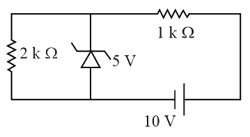 JEE Main/Numerical/Medium/Diodes/With diagram
- 82Two Zener diodes ( and ) having breakdown voltages of and respectively, are connected as shown in the circuit below. The output voltage variation with input voltage linearly increasing with time, is given by ()JEE Main/MCQ/Medium/Diodes
- 83Take the breakdown voltage of the zener diode used in the given circuit as . For the input voltage shown in the figure below, the time variation of the output voltage is: (Graphs drawn are schematic and not to the scale)
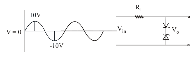 JEE Main/MCQ/Medium/Diodes/With diagram
- 84When a diode is forward biased, it has a voltage drop of . the safe limit of current through the diode is . If a battery of emf is used in the circuit, the value of minimum resistance to be connected in series with the diode so that the current does not exceed the safe limit is :JEE Main/MCQ/Medium/Diodes
- 85In the circuit shown below, is working as a regulated voltage source. When is used as an input, the power dissipated (in ) in each diode is (Considering both zener diodes are identical)
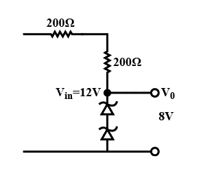 JEE Main/Numerical/Medium/Diodes/With diagram
- 86The current in the network is
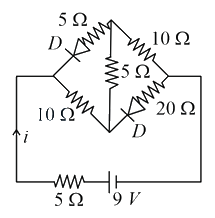 JEE Main/MCQ/Medium/Diodes/With diagram
- 87Both the diodes used in the circuit shown are assumed to be ideal and have negligible resistance when these are forward biased. Built in potential in each diode is . For the input voltages shown in the figure, the voltage (in Volts) at point A is ________
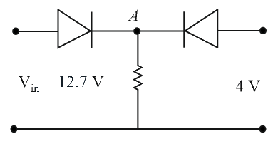 JEE Main/Numerical/Medium/Diodes/With diagram
- 88Figure shows a voltage regulator circuit, with a Zener diode of breakdown voltage . If the unregulated input voltage varies between to then what is the maximum Zener current?
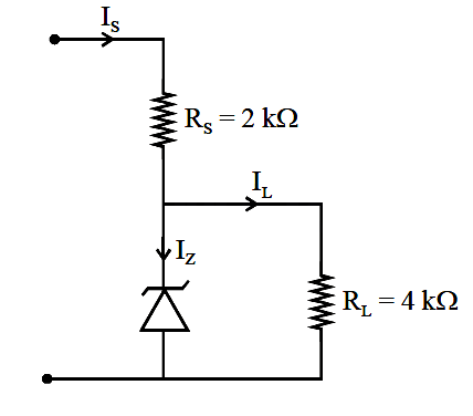 JEE Main/MCQ/Medium/Diodes/With diagram
- 89The figure represents a voltage regulator circuit using a Zener diode. The breakdown voltage of the Zener diode is and the load resistance is, . The series resistance of the circuit is . If the battery voltage varies from to , what are the minimum and maximum values of the current through Zener diode?
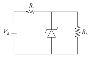 JEE Main/MCQ/Medium/Diodes/With diagram
- 90The reverse break down voltage of a Zener diode is in the given circuit.
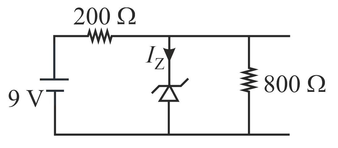
The current through the Zener is:JEE Main/MCQ/Medium/Diodes/With diagram - 91The circuit shown below contains two ideal diodes, each with a forward resistance of . If the battery voltage is the current through the resistance (in Amperes) is:
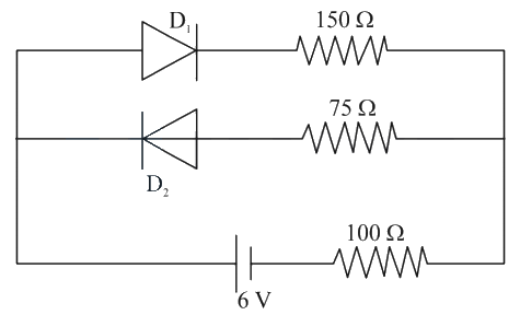 JEE Main/MCQ/Medium/Diodes/With diagram
- 92In the given circuit the current through Zener Diode is close to:
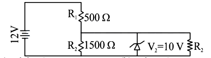 JEE Main/MCQ/Medium/Diodes/With diagram
- 93For the circuit shown below, the current through the Zener diode is
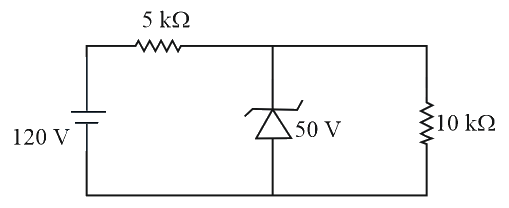 JEE Main/MCQ/Medium/Diodes/With diagram
- 94 and diodes start conducting at and respectively. In the following figure if diode connection are reversed, the value of changes by: (assume that the Ge diode has large breakdown voltage)
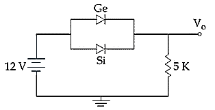 JEE Main/MCQ/Medium/Diodes/With diagram
- 95In the given circuit the current through zener diode is:
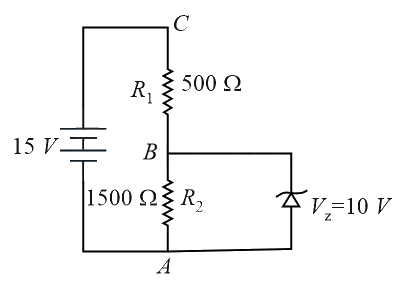 JEE Main/MCQ/Medium/Diodes/With diagram
- 96The reading of the ammeter for a silicon diode in the given circuit is:
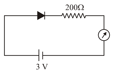 JEE Main/MCQ/Medium/Diodes/With diagram
- 97The characteristic of a diode is shown in the figure. The ratio of forward to reverse bias resistance is:
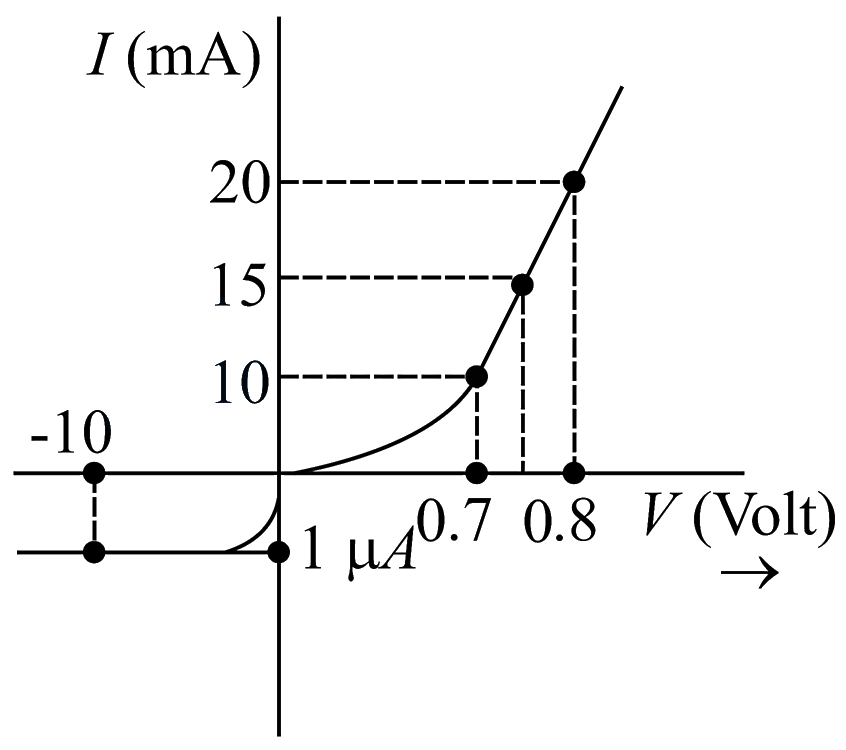 JEE Main/MCQ/Medium/Diodes/With diagram
- 98A Zener diode with a breakdown voltage of is connected in series with a resistance to a battery of emf . The maximum power dissipation rating for the Zener diode is . The value of to ensure maximum power dissipation across the diode isJEE Main/MCQ/Medium/Diodes
- 99Identify the semiconductor devices whose characteristics are given below, in the order :
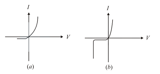
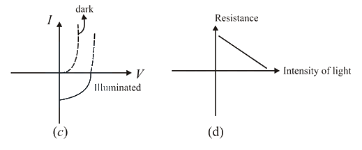 JEE Main/MCQ/Medium/Diodes/With diagram
- 100A battery is connected across as shown in the figure. The value of the current supplied by the battery when in first case battery's positive terminal is connected to and in second case when positive terminal of battery is connected to will respectively be:
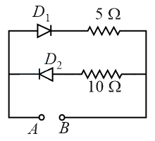 JEE Main/MCQ/Medium/Diodes/With diagram
- 101The value of the resistor, , needed in the DC voltage regulator circuit shown here, equals:
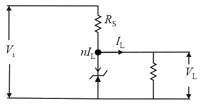 JEE Main/MCQ/Medium/Diodes/With diagram
- 102In an unbiased p - n junction electrons diffuse from n-region to p-region because:JEE Main/MCQ/Medium/Diodes
- 103A Zener diode is connected to a battery and a load as show below:
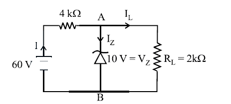
The currents, and are respectively.JEE Main/MCQ/Medium/Diodes/With diagram - 104The forward biased diode connection is :JEE Main/MCQ/Medium/Diodes
- 105Figure shows a circuit in which three identical diodes are used. Each diode has forward resistance of and infinite backward resistance. Resistors . Battery voltage is . The current through is :
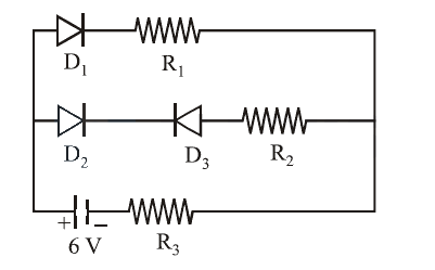 JEE Main/MCQ/Medium/Diodes/With diagram
- 106The characteristics of an is:JEE Main/MCQ/Medium/Diodes
- 107A diode detector is used to detect an amplitude modulated wave of 60% modulation by using a condenser of capacity 250 pico farad in parallel with a load resistance of 100 kilo ohm. Find the maximum modulated frequency which could be detected by it.JEE Main/MCQ/Medium/Diodes
- 108If in a junction diode, a square input signal of is applied as shown

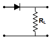
Then the output signal across will beJEE Main/MCQ/Medium/Diodes/With diagram - 109The circuit has two oppositely connect ideal diodes in parallel. What is the current following in the circuit?
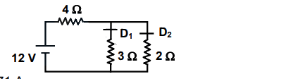 JEE Main/MCQ/Medium/Diodes/With diagram
- 110In the following, which one of the diodes is reverse biased?JEE Main/MCQ/Medium/Diodes
- 111When p-n junction diode is forward biasedJEE Main/MCQ/Medium/Diodes
- 112In the middle of the depletion layer of a reverse biased p-n junction, theJEE Main/MCQ/Medium/Diodes
- 113Two p-n junction diodes and are connected as shown in figure. and are input signals and is the output. The given circuit will function as a .
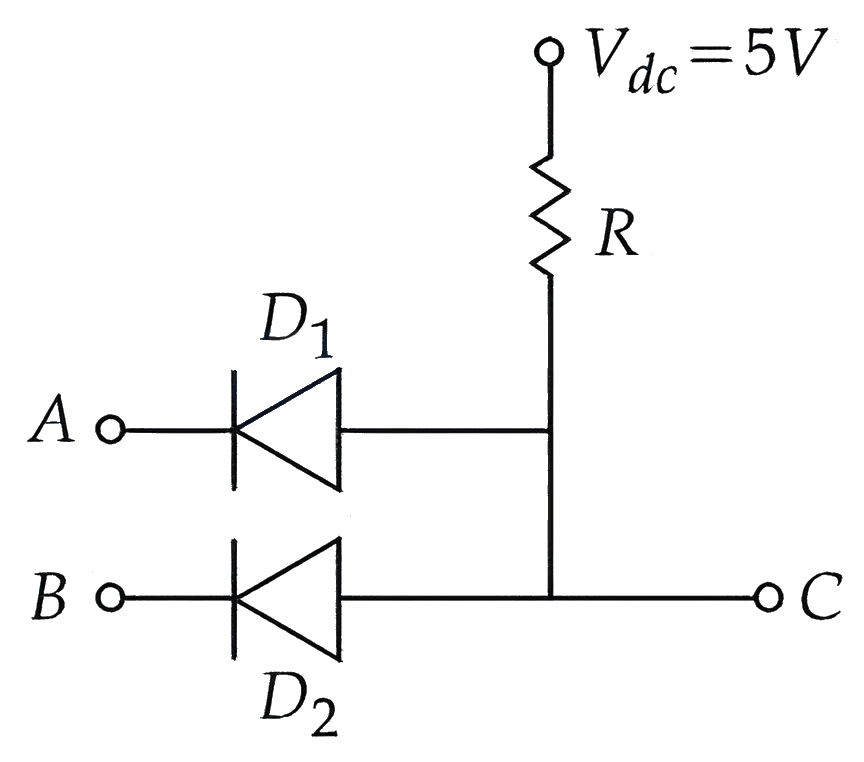 JEE Main/MCQ/Medium/Logic Gates/With diagram
- 114Statement I : To get a steady DC output from the pulsating voltage received from a full wave rectifier we can connect a capacitor across the output parallel to the load
Statement II : To get a steady DC output from the pulsating voltage received from a full wave rectifier we can connect an inductor in series with
In the light of the above statements, choose the most appropriate answer from the options given below :JEE Main/MCQ/Medium/Rectifier - 115A p-n junction (D) shown in the figure can act as a rectifier. An alternating current source is connected in the circuit.
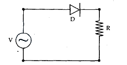 JEE Main/MCQ/Medium/Rectifier/With diagram
- 116In a full wave rectifier circuit operating from mains frequency, the fundamental frequency in the ripple would beJEE Main/MCQ/Medium/Rectifier
- 117Consider the following statements:
A. The junction area of solar cell is made very narrow compared to a photo diode.
B. Solar cells are not connected with any external bias.
C. LED is made of lightly doped p-n junction.
D. Increase of forward current results in continuous increase of LED light intensity.
E. LEDs have to be connected in forward bias for emission of light.
Choose the correct answer from the options given below:JEE Main/MCQ/Medium/Special purpose diodes - 118The characteristics of an electronic device shown in the figure. The device is:
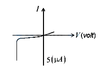 JEE Main/MCQ/Medium/Special purpose diodes/With diagram
- 119Conductivity of a photodiode starts changing only if the wavelength of incident light is less than The band gap of photodiode is found to be The value of is:
(Given )JEE Main/MCQ/Medium/Special purpose diodes - 120Which of the following statement is not correct in the case of light emitting diodes?
A. It is a heavily doped p-n junction.
B. It emits light only when it is forward biased.
C. It emits light only when it is reverse biased.
D. The energy of the light emitted is equal to or slightly less than the energy gap of the semiconductor used.
Choose the correct answer from the options given below :JEE Main/MCQ/Medium/Special purpose diodes - 121Given below are two statements : one is labelled as Assertion A and the other is labelled as Reason R
Assertion A: Photodiodes are used in forward bias usually for measuring the light intensity.
Reason R: For a junction diode, at applied voltage the current in the forward bias is more than the current in the reverse bias for where is the threshold voltage and is the breakdown voltage.
In the light of the above statements, choose the correct answer from the options given belowJEE Main/MCQ/Medium/Special purpose diodes - 122Given below are two statements: one is labelled as Assertion A and the other is labelled as Reason R.
Assertion A: Photodiodes are preferably operated in reverse bias condition for light intensity measurement.
Reason R: The current in the forward bias is more than the current in the reverse bias for a junction diode.
In the light of the above statement, choose the correct answer from the options given below :JEE Main/MCQ/Medium/Special purpose diodes - 123Identify the solar cell characteristics from the following options :JEE Main/MCQ/Medium/Special purpose diodes
- 124The photodiode is used to detect the optical signals. These diodes are preferably operated in reverse biased mode becauseJEE Main/MCQ/Medium/Special purpose diodes
- 125LED is constructed from semiconducting material. The energy gap of this LED is . Calculate the wavelength of light emitted and its colour. and JEE Main/MCQ/Medium/Special purpose diodes
- 126With increasing biasing voltage of a photo diode, the photocurrent magnitude:JEE Main/MCQ/Medium/Special purpose diodes
- 127If a semiconductor photo diode can detect a photon with a maximum wavelength of , then its band gap energy is: Planck's constant
Speed of light JEE Main/MCQ/Medium/Special purpose diodes - 128The output for the given inputs and to the circuit is:
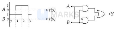 JEE Main/MCQ/Medium/Logic gates/With diagram
- 129Refer to the logic circuit given below. For two inputs and , output will be __________.
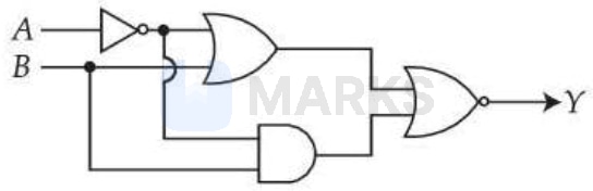 JEE Main/MCQ/Medium/Logic gates/With diagram
- 130For the given logic circuit, which of the following inputs combination will make both LED and LED to glow?
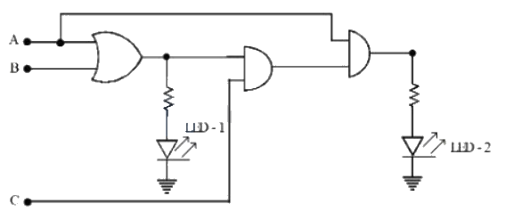 JEE Main/MCQ/Medium/Logic gates/With diagram
- 131Two bits binary numbers, and are given in the inputs of a logic circuit shown in figure below. The output will be:
 JEE Main/MCQ/Medium/Logic gates/With diagram
- 132If and are the inputs, the given circuit works as _______.
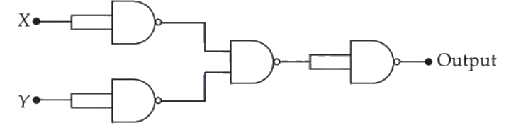 JEE Main/MCQ/Medium/Logic gates/With diagram
- 133Identify the correct truth table of the given logic circuit.
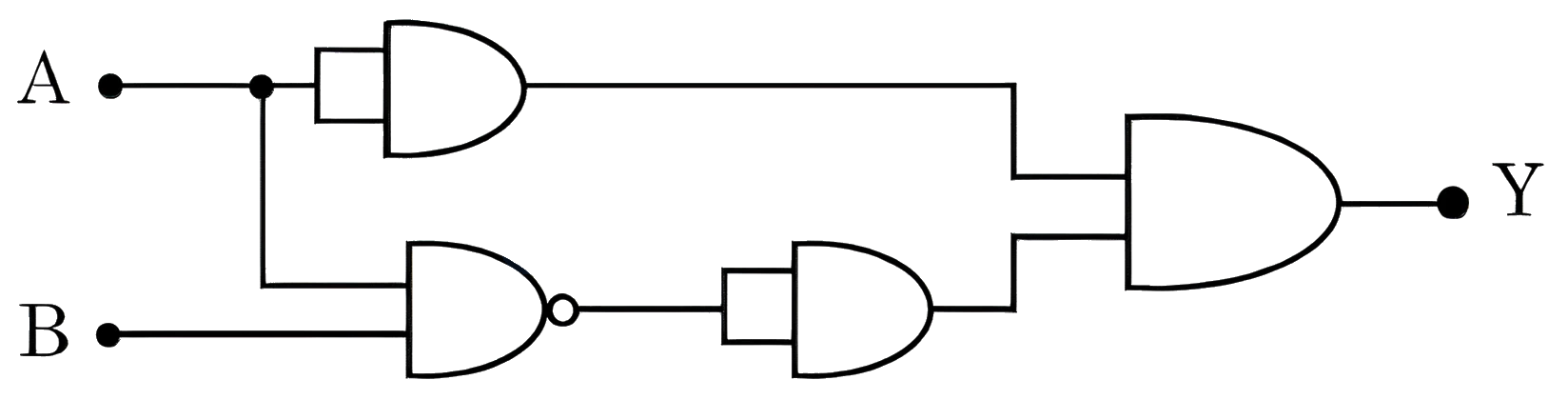 JEE Main/MCQ/Medium/Logic gates/With diagram
- 134For the given logic gate circuit, which of the following is the correct truth table?
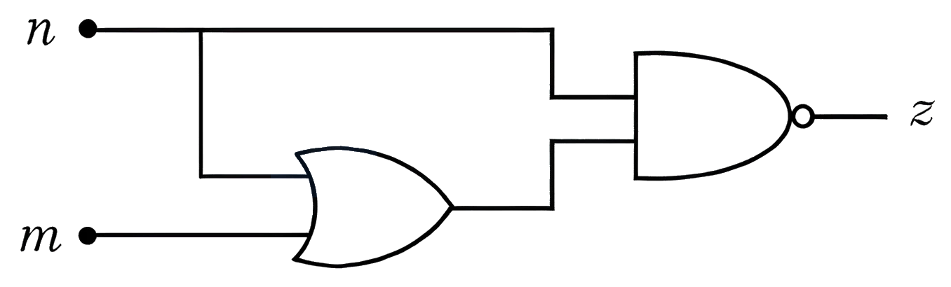 JEE Main/MCQ/Medium/Logic gates/With diagram
- 135The correct truth table for the given input data of the following logic gate is :
Inputs
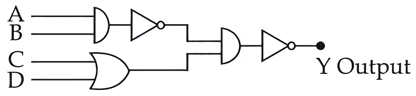 JEE Main/MCQ/Medium/Logic gates/With diagram
- 136Find the correct combination of and D inputs which can cause the LED to glow.
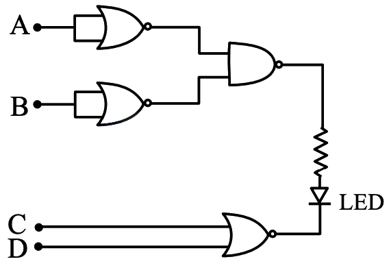 JEE Main/MCQ/Medium/Logic gates/With diagram
- 137The given circuit works as :
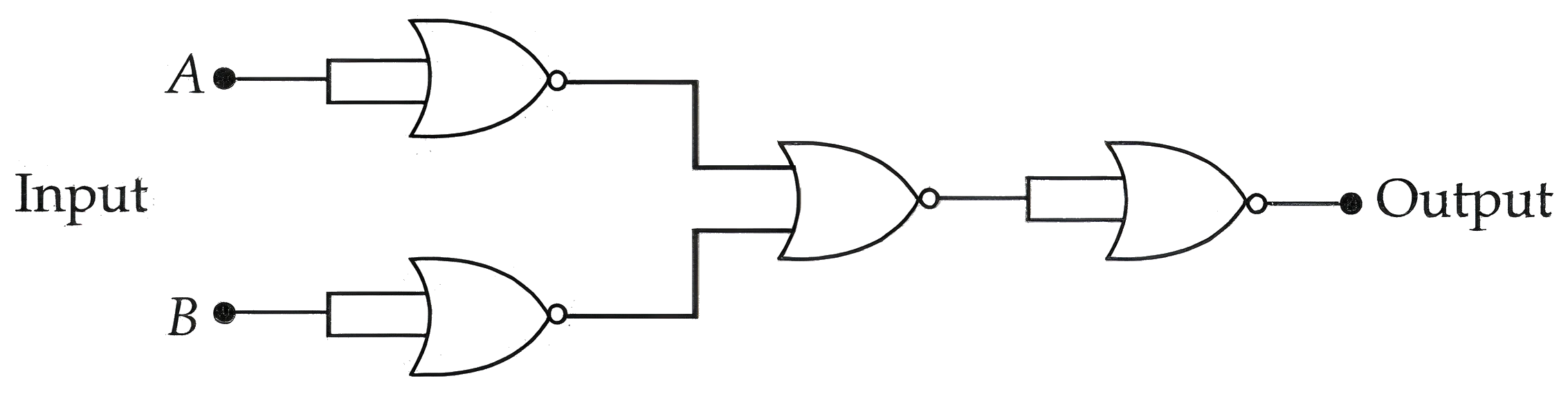 JEE Main/MCQ/Medium/Logic gates/With diagram
- 138Consider the following logic circuit.
The output is when :JEE Main/MCQ/Medium/Logic gates/With diagram - 139The Boolean expression can be realised with which of the following gate configurations.
A. One 3-input AND gate, 3 NOT gates and one 2input OR gate, One 2-input AND gate,
B. One 3-input AND gate, 1 NOT gate, One 2input NOR gate and one 2-input OR gate
C. 3-input OR gate, 3 NOT gates and one 2-input AND gate
Choose the correct answer from the options given belowJEE Main/MCQ/Medium/Logic gates - 140The truth table corresponding to the circuit given below is
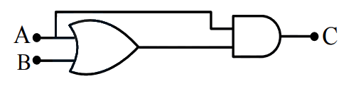 JEE Main/MCQ/Medium/Logic gates/With diagram
- 141Choose the correct logic circuit for the given truth table having inputs A and B.
JEE Main/MCQ/Medium/Logic gates - 142In the digital circuit shown in the figure, for the given inputs the P and Q values are :
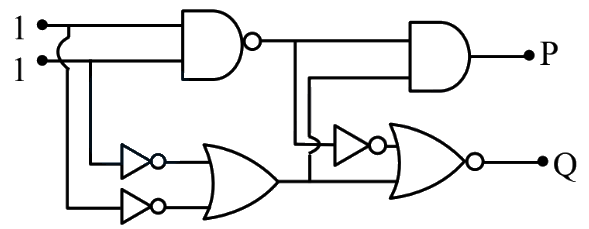 JEE Main/MCQ/Medium/Logic gates/With diagram
- 143The truth table for the circuit given below is :
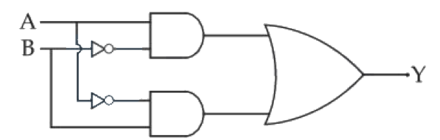 JEE Main/MCQ/Medium/Logic gates/With diagram
- 144
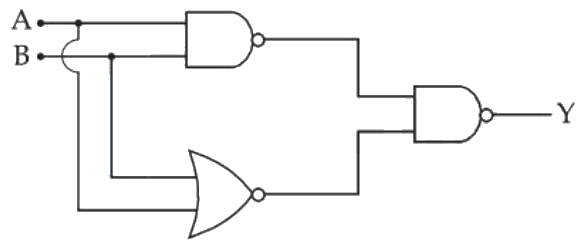
For the circuit shown above, equivalent GATE is :JEE Main/MCQ/Medium/Logic gates/With diagram - 145Which of the following circuits has the same outpur as that of the given circuit?
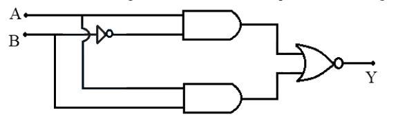 JEE Main/MCQ/Medium/Logic gates/With diagram
- 146The output of the circuit is low (zero) for :

(A)
(B)
(C)
(D)
Choose the correct answer from the options given below :JEE Main/MCQ/Medium/Logic gates/With diagram - 147
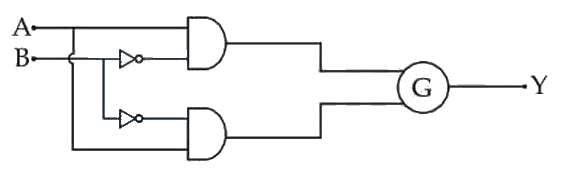
\begin{array}{c|c|c} A & B & Y \\\hline 0 & 0 & 1 \\0 & 1 & 1 \\1 & 0 & 0 \\1 & 1 & 1\end{array}
To obtain the given truth table, following logic gate should be placed at G:JEE Main/MCQ/Medium/Logic gates/With diagram - 148
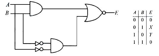
In the truth table of the above circuit the value of and are :JEE Main/MCQ/Medium/Logic gates/With diagram - 149The output of following circuit for given inputs is :
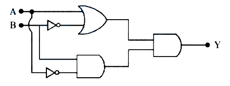 JEE Main/MCQ/Medium/Logic gates/With diagram
- 150The correct truth table for the following logic circuit is :
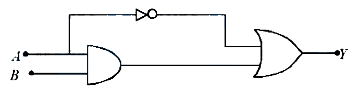 JEE Main/MCQ/Medium/Logic gates/With diagram
- 151The output of logic circuit given below is 0 only when :
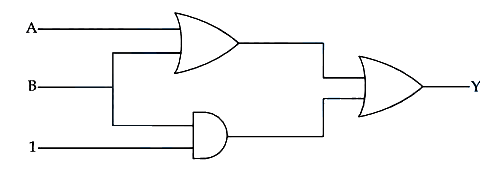 JEE Main/MCQ/Medium/Logic gates/With diagram
- 152Following gates section is connected in a complete suitable circuit.
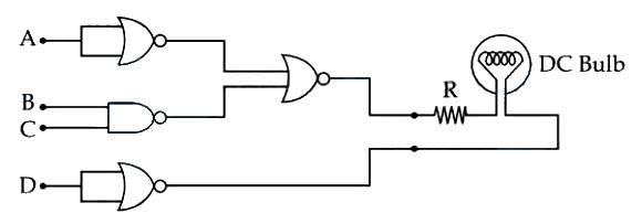
JEE Main/MCQ/Medium/Logic gates/With diagram - 153Identify the logic gate given in the circuit:
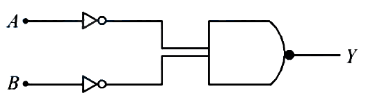 JEE Main/MCQ/Medium/Logic gates/With diagram
- 154The output of the given circuit diagram is
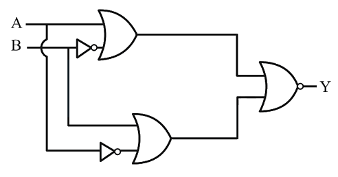 JEE Main/MCQ/Medium/Logic gates/With diagram
- 155Identify the logic operation performed by the given circuit.
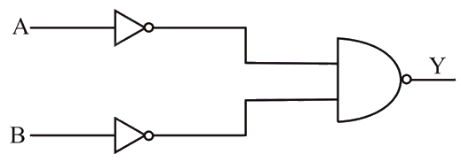 JEE Main/MCQ/Medium/Logic gates/With diagram
- 156The truth table for this given circuit is:
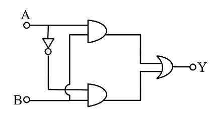 JEE Main/MCQ/Medium/Logic gates/With diagram
- 157The truth table of the given circuit diagram is :
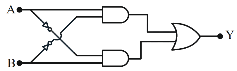 JEE Main/MCQ/Medium/Logic gates/With diagram
- 158The output from a NAND gate having inputs A and B given below will be,
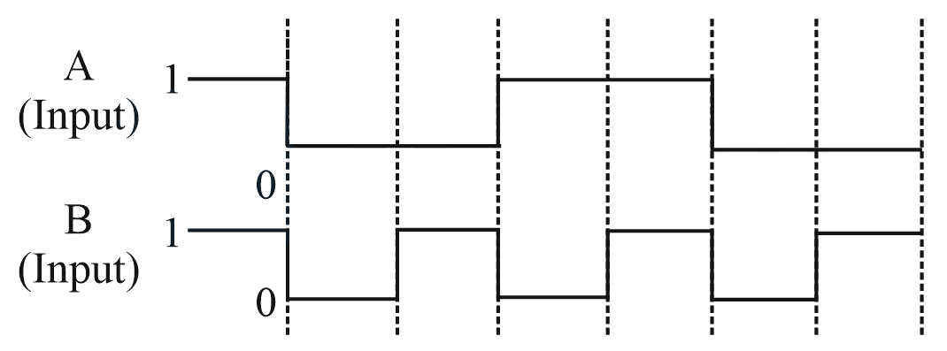 JEE Main/MCQ/Medium/Logic gates/With diagram
- 159For the following circuit and given inputs and choose the correct option for output
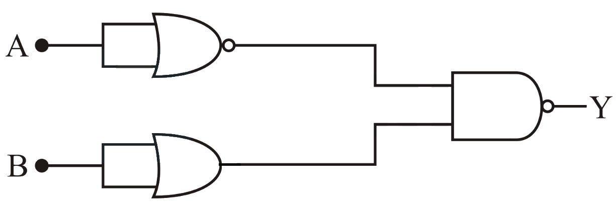
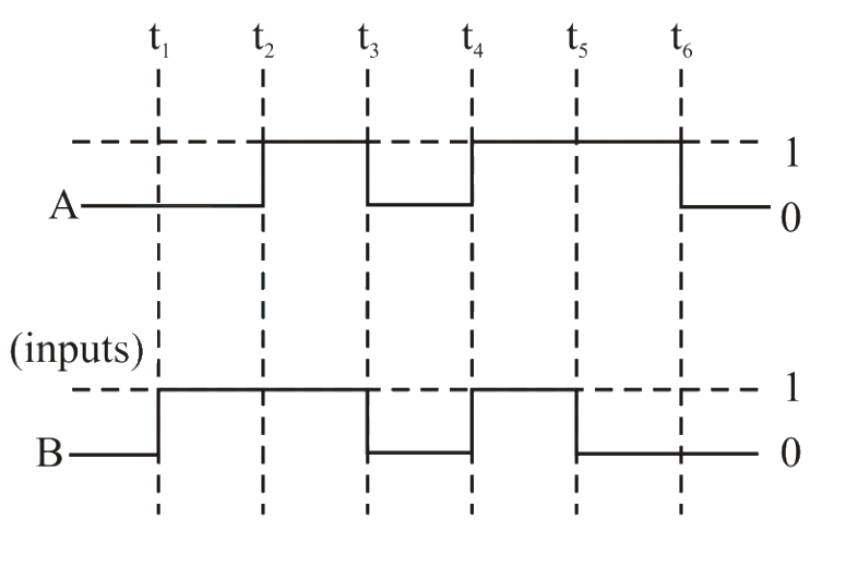 JEE Main/MCQ/Medium/Logic gates/With diagram
- 160The logic operations performed by the given digital circuit is equivalent to:
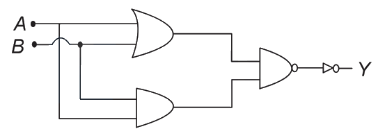 JEE Main/MCQ/Medium/Logic gates/With diagram
- 161The logic performed by the circuit shown in figure is equivalent to
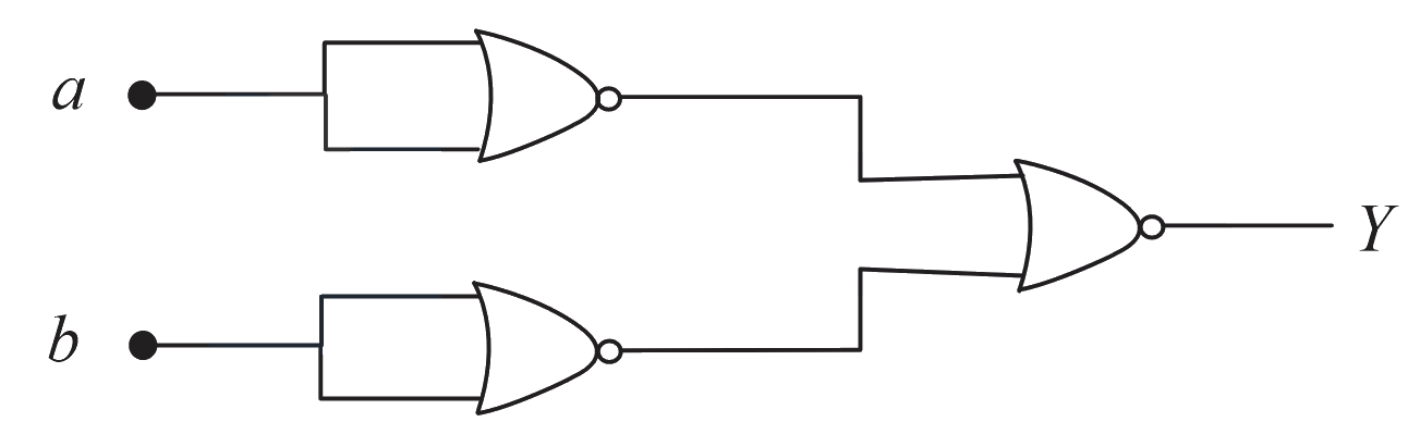 JEE Main/MCQ/Medium/Logic gates/With diagram
- 162For the logic circuit shown, the output waveform at is
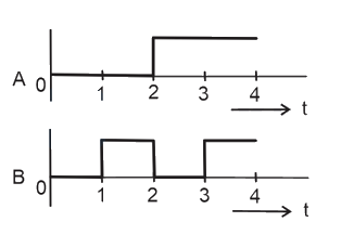
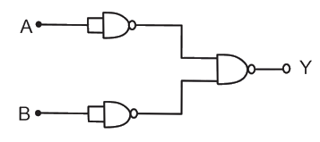 JEE Main/MCQ/Medium/Logic gates/With diagram
- 163Name the logic gate equivalent to the diagram attached
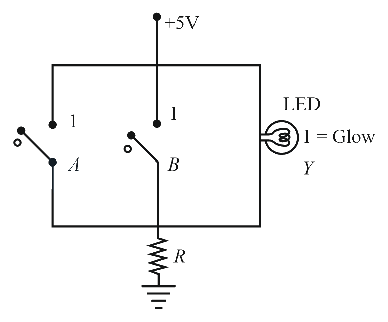 JEE Main/MCQ/Medium/Logic gates/With diagram
- 164The output for the inputs and of circuit is given by
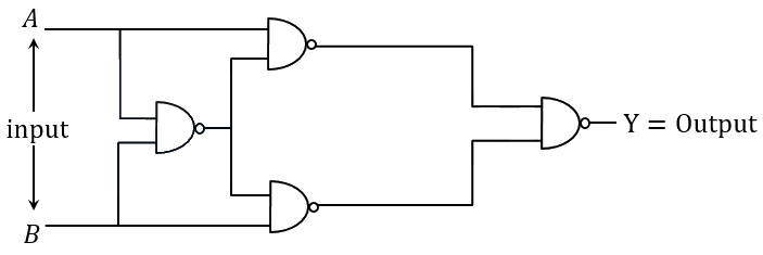
Truth table of the shown circuit is :JEE Main/MCQ/Medium/Logic gates/With diagram - 165The output waveform of the given logical circuit for the following inputs and as shown below, is
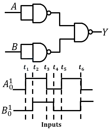 JEE Main/MCQ/Medium/Logic gates/With diagram
- 166For the given logic gates combination, the correct truth table will be
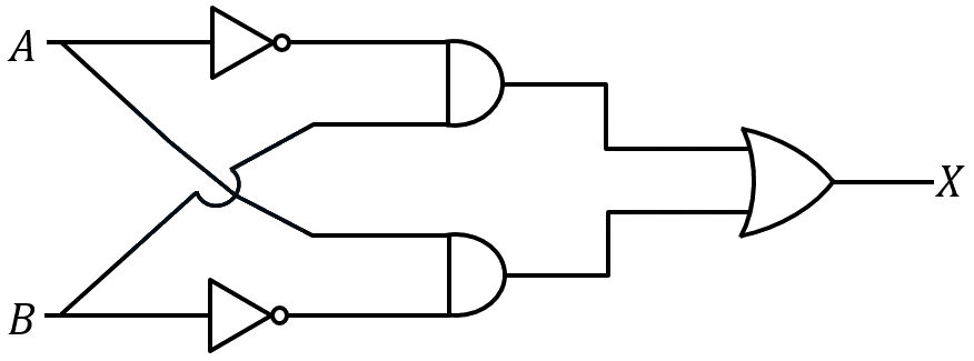 JEE Main/MCQ/Medium/Logic gates/With diagram
- 167The logic gate equivalent to the given circuit diagram is :
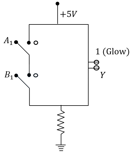 JEE Main/MCQ/Medium/Logic gates/With diagram
- 168A logic gate circuit has two inputs and and output . The voltage waveforms of and are shown below
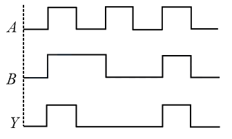
The logic gate circuit isJEE Main/MCQ/Medium/Logic gates/With diagram - 169In the circuit, the logical value of or when potential at or is and the logical value of or when potential at or is .
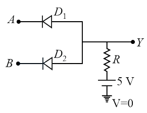
The truth table of the given circuit will be :JEE Main/MCQ/Medium/Logic gates/With diagram - 170Identify the correct Logic Gate for the following output of two inputs and .
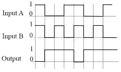 JEE Main/MCQ/Medium/Logic gates/With diagram
- 171Identify the logic operation performed by the given circuit
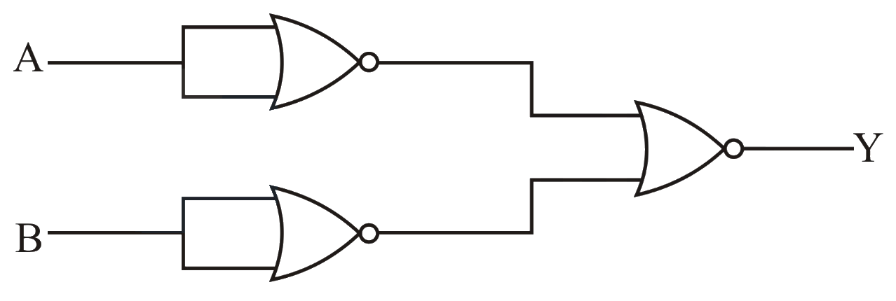 JEE Main/MCQ/Medium/Logic gates/With diagram
- 172In the following logic circuit the sequence of the inputs are and The output for this sequence will be :
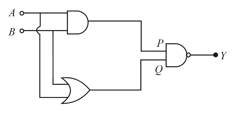 JEE Main/MCQ/Medium/Logic gates/With diagram
- 173Four NOR gates are connected as shown in figure. The truth table for the given figure is :
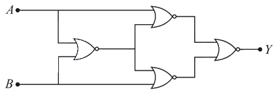 JEE Main/MCQ/Medium/Logic gates/With diagram
- 174Identify the logic operation carried out by the given circuit:
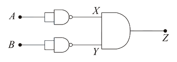 JEE Main/MCQ/Medium/Logic gates/With diagram
- 175Find the truth table for the function of and represented in the following figure.
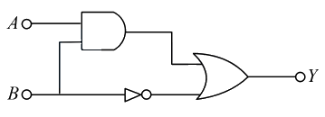 JEE Main/MCQ/Medium/Logic gates/With diagram
- 176Identify the logic operation carried out.
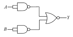 JEE Main/MCQ/Medium/Logic gates/With diagram
- 177Which one of the following will be the output of the given circuit?
 JEE Main/MCQ/Medium/Logic gates/With diagram
- 178The output of the given combination gates represents:
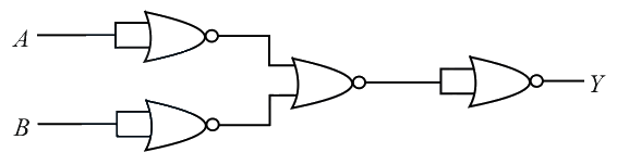 JEE Main/MCQ/Medium/Logic gates/With diagram
- 179The following logic gate is equivalent to :
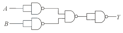 JEE Main/MCQ/Medium/Logic gates/With diagram
- 180In the logic circuit shown in the figure, if input and are to respectively, the output at would be . The value of is _________.
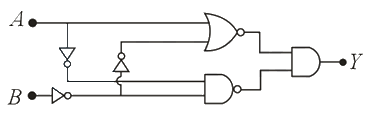 JEE Main/Numerical/Medium/Logic gates/With diagram
- 181Draw the output signal in the given combination of gates.
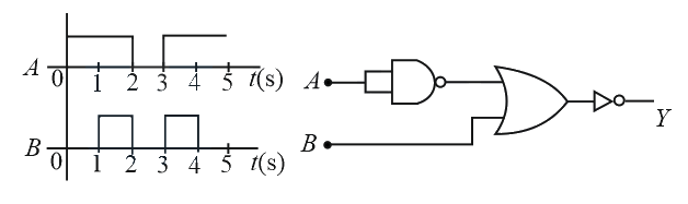 JEE Main/MCQ/Medium/Logic gates/With diagram
- 182The truth table for the following logic circuit is :
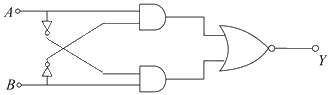 JEE Main/MCQ/Medium/Logic gates/With diagram
- 183
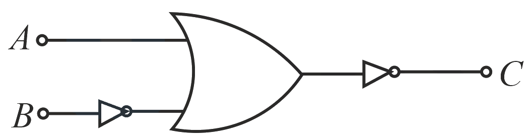
The logic circuit shown above is equivalent to :JEE Main/MCQ/Medium/Logic gates/With diagram - 184Identify the correct output signal in the given combination of gates (as shown ) for the given inputs
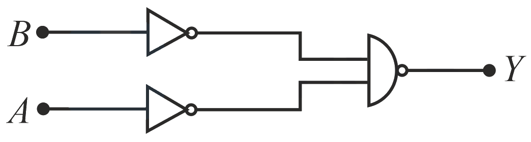
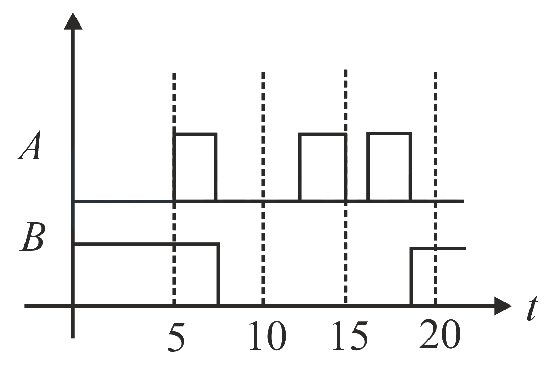 JEE Main/MCQ/Medium/Logic gates/With diagram
- 185Identify the operation performed by the circuit given below :
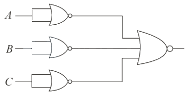 JEE Main/MCQ/Medium/Logic gates/With diagram
- 186In the following, digital circuit, what will be the output a '', when the input are
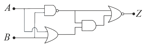 JEE Main/MCQ/Medium/Logic gates/With diagram
- 187In the given circuit, value of is:
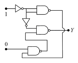 JEE Main/MCQ/Medium/Logic gates/With diagram
- 188Boolean relation at the output stage- for the following circuit is:
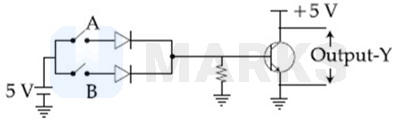 JEE Main/MCQ/Medium/Logic gates/With diagram
- 189Which of the following gives a reversible operation?JEE Main/MCQ/Medium/Logic gates
- 190The truth table for the circuit given in the figure is:
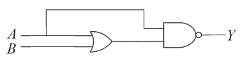 JEE Main/MCQ/Medium/Logic gates/With diagram
- 191The logic gate equivalent to the given logic circuit is:
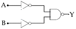 JEE Main/MCQ/Medium/Logic gates/With diagram
- 192The output of the given logic circuit is:
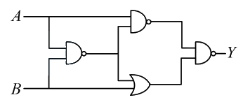 JEE Main/MCQ/Medium/Logic gates/With diagram
- 193To get output '1' at for the given logic gate circuit the input values must be:
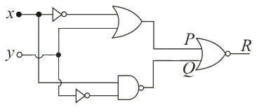 JEE Main/MCQ/Medium/Logic gates/With diagram
- 194Truth table for the given circuit will be
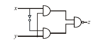 JEE Main/MCQ/Medium/Logic gates/With diagram
- 195To get an output of from the circuit shown in the figure the input must be:
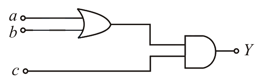 JEE Main/MCQ/Medium/Logic gates/With diagram
- 196The truth table given in fig. represents: A B Y 0 0 0 0 1 1 1 0 1 1 1 1JEE Main/MCQ/Medium/Logic gates
- 197If a, b, c, d are inputs to a gate and is its output, then, as per the following time graph, the gate is:
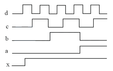 JEE Main/MCQ/Medium/Logic gates/With diagram
- 198
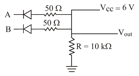
Given, and are input terminals
Logic is
Logic is
Which logic gate operation, the following circuit does?
Note: This question was awarded a bonus. option changed.JEE Main/MCQ/Medium/Logic gates/With diagram - 199Identify the gate and match in the bracket to check.
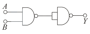 JEE Main/MCQ/Medium/Logic gates/With diagram
- 200Which of the following circuits correctly represents the following truth table ?
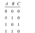 JEE Main/MCQ/Medium/Logic gates/With diagram
- 201A system of four gates is set up as shown. The 'truth table' corresponding to this system is :
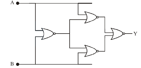 JEE Main/MCQ/Medium/Logic gates/With diagram
- 202Consider two npn transistors as shown in figure. If 0 Volts corresponds to false and 5 Volts correspond to true then the output at C corresponds to :
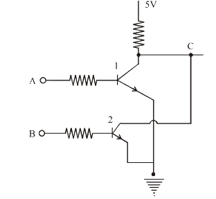 JEE Main/MCQ/Medium/Logic gates/With diagram
- 203The figure shows a combination of two NOT gates and a NOR gate.
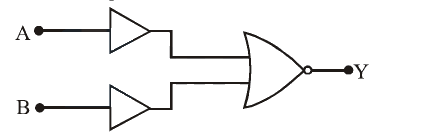
The combination is equivalent to JEE Main/MCQ/Medium/Logic gates/With diagram - 204Which one of the following is the Boolean expression for NOR gate?JEE Main/MCQ/Medium/Logic gates
- 205Which logic gate with inputs and performs the same operation as that performed by the following circuit?
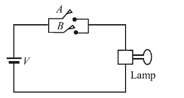 JEE Main/MCQ/Medium/Logic gates/With diagram
- 206Truth table for system of four NAND gates as shown in figure is
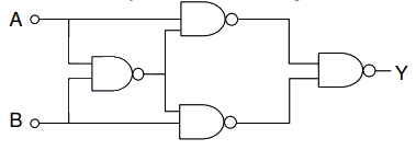 JEE Main/MCQ/Medium/Logic gates/With diagram
- 207The combination of gates shown below yields
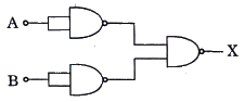 JEE Main/MCQ/Medium/Logic gates/With diagram
- 208The logic circuit shown below has the input waveforms 'A' and 'B' as shown. Pick out the correct output waveform.
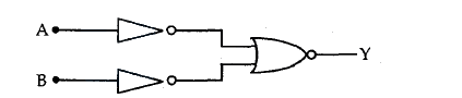
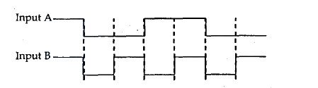 JEE Main/MCQ/Medium/Logic gates/With diagram
- 209In the circuit below, and represent two inputs and represents the output. The circuit represents
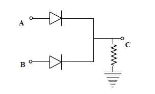 JEE Main/MCQ/Medium/Logic gates/With diagram
NEET question paper PDF
This chapter includes NEET questions. Open a year to read the full paper, or download the PDF.
Opening paper…
JEE Main question paper PDF
This chapter includes JEE Main questions. Open a shift to read the paper, or download the PDF.
Opening paper…
Other Physics chapters
Current Electricity 380Electrostatics 311Kinematics 308Ray Optics 295Rotational Motion 280Magnetic Effects & Magnetism 276Atoms & Nuclei 239Gravitation 223Laws of Motion 210Dual Nature of Matter 200Oscillations 194Fluid Mechanics 192Wave Optics 191Alternating Current 190Thermodynamics 190Work Energy Power 183Capacitors 180Kinetic Theory 168Electromagnetic Waves 165Electromagnetic Induction 153Units & Dimensions 149Waves 142Center of Mass, Momentum & Collision 130Thermal Properties of Matter 126Mathematics in Physics 121Mechanical Properties of Solids 118Experimental Physics 70Magnetic Properties of Matter 57Modern Physics 5
Stuck on a Semiconductors question from your book?
Snap it and get a whiteboard video that solves it step by step. Your first video needs no login.