Semiconductors

JEE Main level, single correct, medium

162 of 209

Question 162 of 209

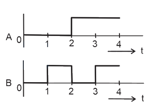
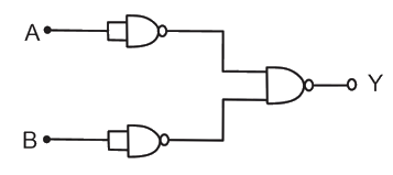
For the logic circuit shown, the output waveform at YY is

Show answer and solution

Answer: (A)
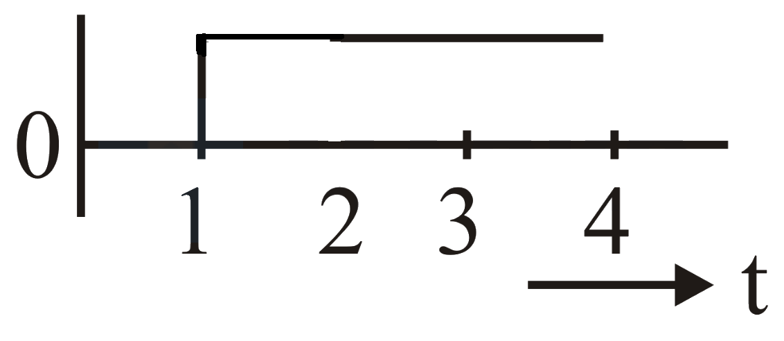
All the gates used in the diagram represent NAND gates.
Thus, the output
YY can be calculated as follows
Y=A⋅B=A+B=A+B\begin{matrix}Y & = & A\cdot B \\ & = & A+B \\ & = & A+B\end{matrix}
The above equation suggests that the output of the given combination yields the same result as an OR gate.

The truth table can be written as follows
AA BB AA BB Y=A⋅BY=A\cdot B 00 00 11 11 00 00 11 11 00 11 11 00 00 11 11 11 11 00 00 11 Hence, this is the correct output.

JEE Main question paper PDF

Open a shift to read the full paper on this page, or download it.

JEE Main 2025 Apr 2 Shift 1 question paper

Open Download PDF

Opening paper…

Explain it as a whiteboard videoStep-by-step, in Hinglish or English. Your first video needs no login.Solved it on paper but got it wrong?Upload a photo of your working. Mistake Doctor marks the exact line that broke.
See it move: Semiconductors, diodes and logic gates simulationDrag the sliders and watch the numbers in this question change.

More Physics practice

JEE Main Physics practice question on Semiconductors (Logic gates), with the answer and a step-by-step solution. Scan a question from your own book or paper to get a whiteboard video.